Photomasks
Photomasks explained
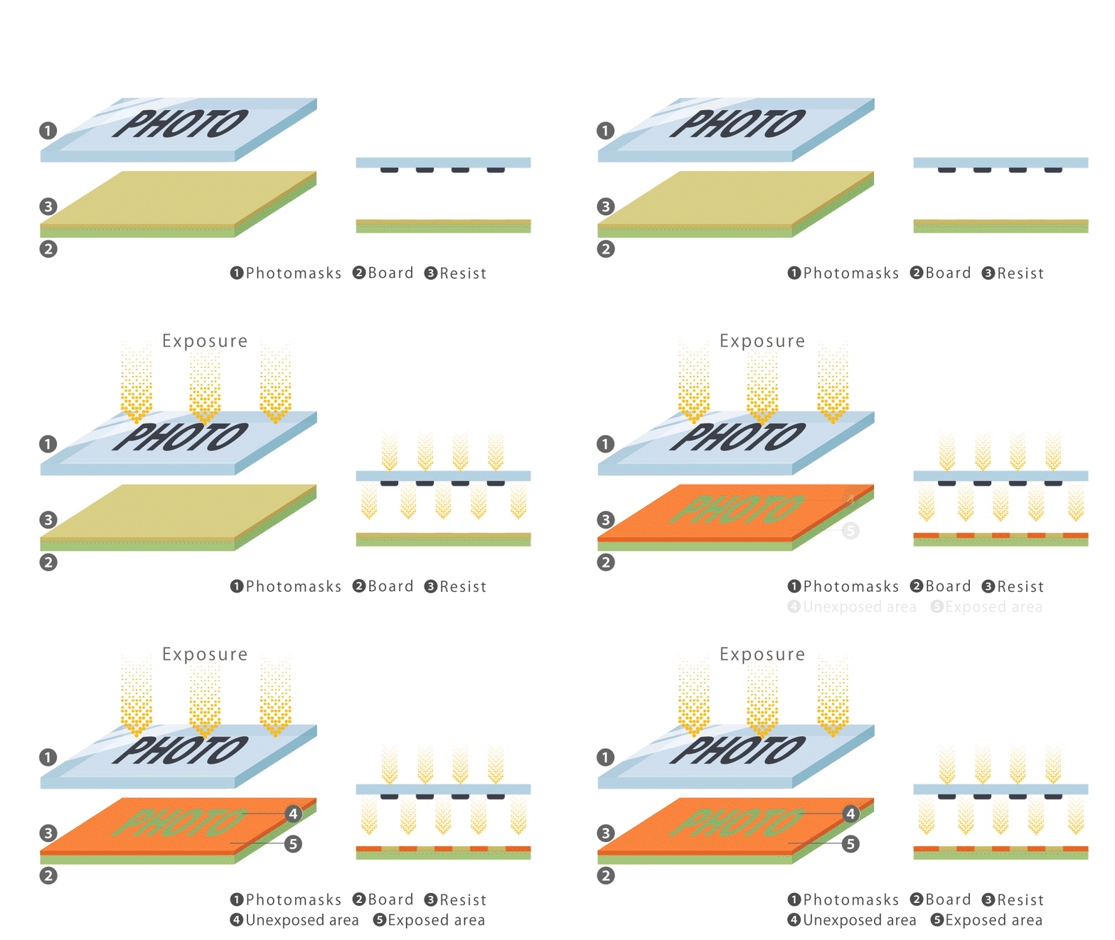
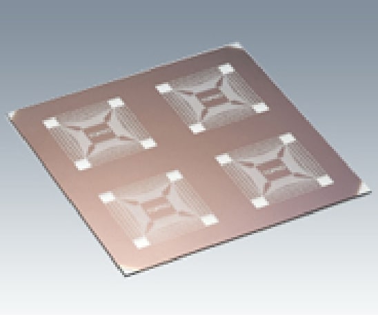
- A photomask is a PET or glass substrate that serves as a base plate for patterning used in the manufacture of electronic components (semiconductors), printed circuit boards, MEMS, and other products.
- It serves as a base plate for transferring electronic components and circuit patterns on printed circuit boards using a transfer technology called photolithography.
- Photomasks are used in a wide range of fields, including printed circuit boards such as PWBs and FPCs, IC packaging, display devices such as LCDs and touch panels, and semiconductor-related electronic components.
Features of photomask manufacturing

Quality assurance of high precision photomask products
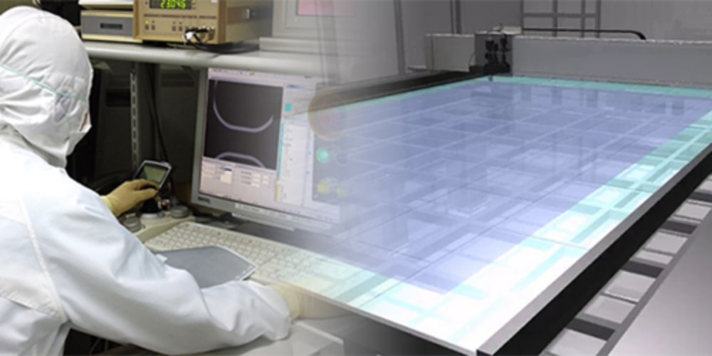
We use the FPD total pitch measurement system for total pitch measurement and inspection of photomask products. We provide quality improvement, quality assurance, and stable quality products around high precision photomasks.

A production system that enables quick delivery
For chrome mask production, we offer a 24-hour manufacturing system that enables us to deliver in the shortest possible time.
Film masks
A basic mask with excellent cost performance. In addition, its polyester base makes it lightweight and flexible for easy handling.
Main applications
Used for PWB, FPC, electronic components, graphics, etc.
Features
- This is the most cost-effective type of photomask.
- Since it is polyester based, it is lightweight, flexible, and easy to work with.
- We can provide detailed support early on from the data editing stage.
- We support fine patterns of about 30 µm.
Supported data
Gerber(274D/274X) / DWG / DXF / GDS2 /ODB++
※We also offer methods of sending and receiving data confidentially,so please contact us.
Optional
Supports laminate film attachment
Standards and specifications
| Substrate | Polyester |
|---|---|
| Supported sizes | ~711x813mm |
| Material thickness | 175μm |
| Film quality | Silver salt gelatin emulsion |
| Film thickness | 7~8μm |
| Minimum lines | 30μm |
|---|---|
| Short dimension accuracy | ±3.0μm~ |
| Long dimension accuracy | ±20.0μm~ |
*Please contact us for sizes other than those listed above.
Emulsion glass masks
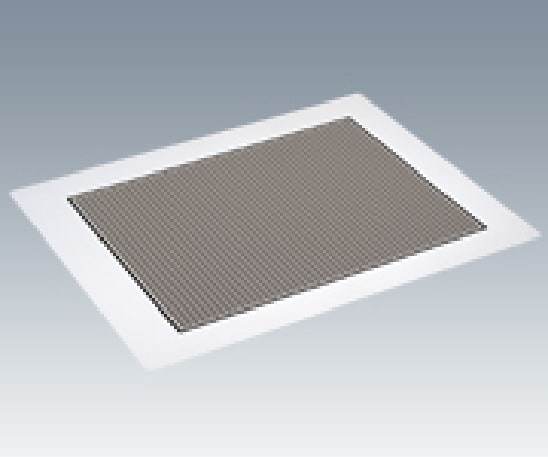
We use high-resolution emulsions for our photomasks, and being glass-based, they feature higher dimensional stability than film masks.
Main applications
FPD (LCD/OLED), electronic components, packaging, etc.
Features
- Glass-based masks have higher dimensional stability than film masks.
- Fine silver particles have less fringing and excellent resolving power.
- We can provide detailed support early on from the data editing stage.
- A high-resolution emulsion supporting fine patterns of about 20μm.
※Patterns of under 20μm may be possible depending on conditions. Please do not hesitate to contact us.
Supported data
Gerber(274D/274X) / DWG / DXF / GDS2/ODB++
※We also offer methods of sending and receiving data confidentially,so please contact us.
Optional
Compatible with hard coatings
Standards and specifications
| Substrate | Soda lime |
|---|---|
| Supported sizes | ~711x813mm |
| Material thickness | 1.8mm~5.0mm |
| Film quality | Silver salt gelatin emulsion |
| Film thickness | 5~6μm |
| Minimum lines | 10μm~ |
|---|---|
| Short dimension accuracy | ±1.0μm~ |
| Long dimension accuracy | ±3.0μm~ |
*Please contact us for sizes other than those listed above.
Chrome glass masks
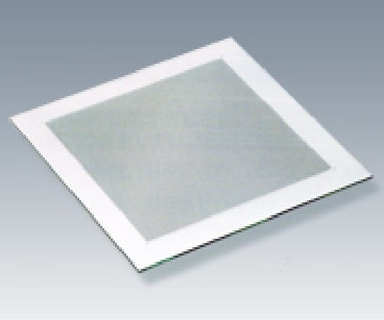
High-spec glass masks that meet all requirements for high definition and high precision Using synthetic quartz material allows for stabilizing the dimensions against temperature changes during exposure. A high-definition mask that can handle up to a minimum pattern width of 2μm.
Main applications
MEMS, LCD, OLED, WLP, thin film chip components, etc.
Features
- Suitable for ultra-high definition imaging due to the lack of fringing.
- Using synthetic quartz material allows for stabilizing the dimensions against temperature changes during exposure.
- Excellent transfer performance due to thin light-shielding film thickness
- Available up to 2μm minimum pattern width
Supported data
Gerber(274D/274X) / DWG / DXF / GDS2/ODB++
※We also offer methods of sending and receiving data confidentially,so please contact us.
Optional
Compatible with thin-film water and oil repellent coatings and hard coatings
Standards and specifications
| Substrate | Soda lime/synthetic quartz |
|---|---|
| Supported sizes | ~700x800mm |
| Material thickness | 1.0mm~5.0mm |
| Film quality | Low reflection 2-layer chrome/ single layer chrome/3-layer chrome |
| Film thickness | 100~125nm |
| Minimum lines | 2μm~ |
|---|---|
| Short dimension accuracy | ±0.2μm~ |
| Long dimension accuracy | ±0.5μm~ |
*Please contact us for sizes other than those listed above.
Substrate comparison table
Substrate/manufacturing standard
Film masks
Emulsion glass masks
Chrome glass masks
Substrate standard
Substrate
Polyester
Soda lime
Soda lime/synthetic quartz
Substrate thickness
175μm
1.8~5.0mm
1.0~5.0mm
Film quality
Silver salt gelatin emulsion
Silver salt gelatin emulsion
Low reflection 2-layer chrome/single-layer chrome/3-layer chrome
Film thickness
7~8μm
5~6μm
100~125nm
Supported sizes
~711×813mm
~711×813mm
~700×800mm
Rendering area
~690×800mm
~680×780mm
~700×800mm
Manufacturing standards
Minimum lines
30μm
10μm
2μm
Short dimension accuracy
±3μm~
±1μm~
±0.2μm~
Long dimension accuracy
±20μm~
±3μm~
±0.5μm~
| Film masks | Emulsion glass masks | Chrome glass masks | ||
|---|---|---|---|---|
| Substrate standard | Substrate | Polyester | Soda lime | Soda lime/synthetic quartz |
| Substrate thickness | 175μm | 1.8~5.0mm | 1.0~5.0mm | |
| Film quality | Silver salt gelatin emulsion | Silver salt gelatin emulsion | Low reflection 2-layer chrome/single-layer chrome/3-layer chrome | |
| Film thickness | 7~8μm | 5~6μm | 100~125nm | |
| Supported sizes | ~711×813mm | ~711×813mm | ~700×800mm | |
| Rendering area | ~690×800mm | ~680×780mm | ~700×800mm | |
| Manufacturing standards | Minimum lines | 30μm | 10μm | 2μm |
| Short dimension accuracy | ±3μm~ | ±1μm~ | ±0.2μm~ | |
| Long dimension accuracy | ±20μm~ | ±3μm~ | ±0.5μm~ | |
Image quality comparison (30µm)
Film masks
Emulsion glass masks
Chrome glass masks
Image
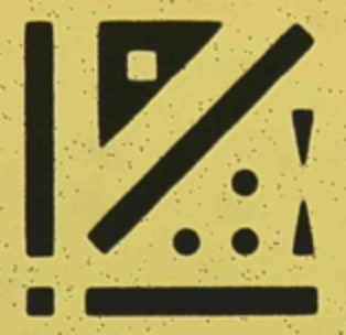
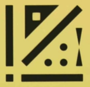
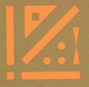
| Film masks | Emulsion glass masks | Chrome glass masks | |
|---|---|---|---|
| Image |  |
 |
 |
Elasticity of each substrate
Polyester
Soda lime
Synthetic quartz
Temperature
Elasticity
0.001%
0.00085%
0.00006%
1 meter equivalent
10.0μm/℃
8.5μm/℃
0.6μm/℃
Wetness
Elasticity
0.0015%
No
No
1 meter equivalent
15.0μm/%
No
No
| Polyester | Soda lime | Synthetic quartz | |||
|---|---|---|---|---|---|
| Temperature | Elasticity | 0.001% | 0.00085% | 0.00006% | |
| 1 meter equivalent | 10.0μm/℃ | 8.5μm/℃ | 0.6μm/℃ | ||
| Wetness | Elasticity | 0.0015% | No | No | |
| 1 meter equivalent | 15.0μm/% | No | No | ||
We can manufacture various types of masks starting from a single sheet.
Are you looking to have a single prototype piece made? We are equipped to flexibly accommodate small lot orders and other requests. Please do not hesitate to contact us.

